The in-plane coefficient of thermal expansion (CTE) of a flip-chip substrate is a decisive material parameter that controls solder bump stress, package warpage, and long-term thermo-mechanical reliability. This article presents a complete technical guide to the flip-chip substrate in-plane CTE experiment, covering sample preparation, test conditions, evaluation methods based on standards such as ASTM E831, ISO 11359-2, and IPC-TM-650, typical experimental results, and how the measured data are applied in package design and reliability assessment by accredited third-party laboratories.
Technical Overview
Flip-chip packaging interconnects a silicon die directly to a substrate through an array of solder bumps, and the thermomechanical compatibility of the die–substrate pair determines the fatigue life of those joints. Silicon exhibits a low linear CTE of approximately 2.6 ppm/°C, whereas organic flip-chip substrates typically expand at 10–20 ppm/°C below the glass transition temperature (Tg) and far more rapidly above Tg. During solder reflow, power cycling, and temperature-cycling tests such as those defined in JESD22-A104, this mismatch imposes cyclic shear strain on every bump, eventually nucleating cracks at the bump–pad interfaces.
The in-plane (X–Y direction) CTE, denoted alpha, is defined as the fractional change in length per unit temperature change, mathematically expressed as alpha = (1/L0) × (dL/dT). Accurate in-plane CTE data are essential inputs for warpage simulation (for example, in support of JESD22-B112 flatness measurements), solder fatigue modeling (Coffin–Manson type lifetime equations), underfill selection, and substrate material qualification. Because the property changes sharply at Tg, a well-designed experiment reports both the pre-Tg segment (alpha1) and the post-Tg segment (alpha2), together with the Tg value itself.
Testing Samples
Organic Laminate Core Substrates
Bismaleimide triazine (BT) and high-Tg epoxy glass core substrates used in conventional flip-chip ball grid array (FC-BGA) packages are the most frequently tested sample type. Specimens are cut as rectangular strips along both the machine direction (X) and the transverse direction (Y) to reveal weave-induced anisotropy, with typical strip dimensions of 6–10 mm in length, 3–4 mm in width, and 0.2–0.8 mm in thickness.
Build-Up and Modified Semi-Additive Process (mSAP) Substrates
Fine-line substrates for high-density flip-chip devices use sequentially deposited epoxy or phenolic-hardened build-up dielectric layers with copper redistribution wiring. These films exhibit higher CTE values than the core, so the experiment is often performed both on the composite finished substrate and on free-standing dielectric film to decouple the film and copper contributions.
Flexible and Polyimide-Based Substrates
Polyimide flex substrates and rigid-flex boards for wafer-level and chip-scale flip-chip packages are tested over wider temperature windows, often from -55 °C to 260 °C, because they experience more extreme use conditions.
Ceramic, Glass, and Silicon Interposer Substrates
Alumina, aluminum nitride, glass cores, and silicon interposers have very low expansion (0.5–8 ppm/°C) and require higher-sensitivity instrumentation such as push-rod dilatometry or laser interferometry to resolve differences below 1 ppm/°C.
Testing Items
A typical flip-chip substrate in-plane CTE experiment report contains the following measured and derived quantities:
- Alpha1 — average in-plane CTE below Tg, normally regressed over a defined window such as 50–150 °C or 30–100 °C.
- Alpha2 — average in-plane CTE above Tg, normally regressed from Tg + 20 °C up to the maximum test temperature.
- Glass transition temperature (Tg) determined from the inflection point of the expansion curve, cross-checkable with DSC per ISO 11357-2 or ASTM D3418 and DMA per ASTM D4065.
- X-direction versus Y-direction CTE comparison to quantify in-plane anisotropy caused by glass weave.
- Percent linear expansion over the full scan range and the total expansion through reflow-relevant temperatures (for example, 25 °C to 245 °C or 260 °C).
- Thermal hysteresis between the first and second heating runs, an indicator of residual stress, moisture history, and cure completion.
- Dimensional stability after thermal exposure, relevant to routing registration and bump alignment.
Testing Methods
Thermomechanical Analysis (TMA) Method
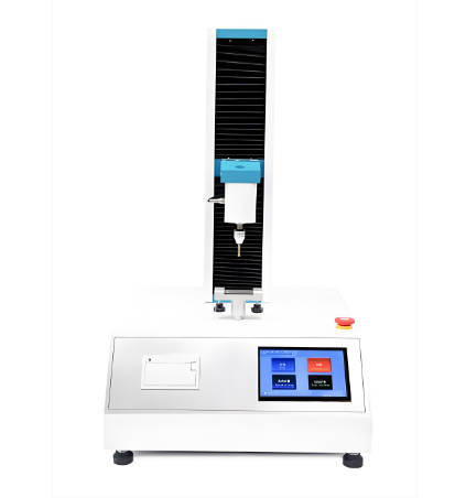
The primary technique is thermomechanical analysis performed in expansion mode in accordance with ASTM E831, ISO 11359-2, and IPC-TM-650 method 2.4.24.4 for X–Y axis expansion. A specimen is placed between a quartz platform and a low-force quartz probe, a small static load (typically 0.05 N or less for thin substrates) is applied, and the length change is tracked by an LVDT or optical encoder while the furnace ramps at 5 °C/min under nitrogen purge. Two consecutive heating runs are common: the first run erases thermal and moisture history, and the second run provides the reported CTE and Tg values.
Push-Rod Dilatometry Method
For thicker cores, ceramic substrates, and interposers with very low expansion, horizontal or vertical dilatometers per ASTM E228 provide superior baseline stability. Calibration is performed against a certified reference material such as fused silica or platinum, and measurement uncertainty below ±0.3 ppm/°C is achievable.
Optical Full-Field Methods
Digital image correlation (DIC) and laser interferometric techniques map CTE across the entire substrate surface, exposing local variations near copper-dense regions, plated through-holes, and buried vias that a strip specimen cannot capture. These methods are increasingly used for build-up substrates where copper pattern density strongly modulates effective expansion.
Specimen Preparation and Conditioning
Recommended practice for consistent results includes the following controls:
- Cut 3 to 5 replicate strips per direction per material lot; deburr edges and verify flatness.
- Bake specimens at 105–125 °C for 1–2 hours to remove absorbed moisture, or apply documented conditioning per ASTM D618 / IPC-TM-650 2.6.2.2 where moisture sensitivity is being evaluated.
- Measure initial length at 23 ± 2 °C with a calibrated micrometer or optical comparator; this L0 anchors all CTE calculations.
- Select the temperature range to mirror the application: 25 °C to 150 °C for operating-life assessment, or 25 °C to 260 °C to cover lead-free reflow excursions.
- Compute alpha by linear regression of the expansion curve over the specified windows and report values in ppm/°C with the regression interval, heating rate, and run number clearly stated.
Typical Experimental Results
Representative values for common flip-chip substrate constructions are as follows: BT/epoxy glass cores show alpha1 of 13–16 ppm/°C and alpha2 of 40–60 ppm/°C with Tg near 180–220 °C by TMA; epoxy build-up dielectric films show alpha1 of 25–45 ppm/°C; polyimide films show 15–25 ppm/°C below Tg; alumina substrates show 6–7 ppm/°C; and silicon interposers match the die at approximately 2.6 ppm/°C. Acceptance specifications from package designers commonly require alpha1 within a defined band (for example, 14–17 ppm/°C) and Tg above a stated minimum to guarantee reflow-dimensional stability.
Applications
- Substrate material qualification and vendor-to-vendor comparison during new package introduction.
- Finite element warpage prediction to meet coplanarity and JESD22-B112 flatness requirements for surface-mount assembly.
- Solder bump fatigue life estimation, where in-plane CTE mismatch drives the plastic strain amplitude in Coffin–Manson and energy-based lifetime models.
- Underfill and capillary adhesive selection, since effective stress transfer requires matching the underfill CTE to the substrate–die system.
- Reflow and bonding process optimization, including bonding force, temperature ramp, and die-attach profile tuning.
- Failure analysis support, comparing the CTE of failed lots against golden reference lots when bump cracking or delamination occurs after thermal cycling.
- Design-rule development for heterogeneous integration, 2.5D interposers, and fan-out panel-level packaging where multi-material stacks demand matched expansion behavior.
FAQ
Why is in-plane CTE measured separately from z-axis CTE? The in-plane mismatch against the silicon die governs bump shear and warpage, while the z-axis expansion controls plated hole and via reliability. IPC-TM-650 method 2.4.24 addresses the z-axis, whereas method 2.4.24.4 addresses the X–Y expansion tested here; both should be characterized for a complete substrate datasheet.
What temperature range should be chosen? For reliability engineering, 25 °C to 260 °C covering lead-free reflow is standard; for in-service behavior, 25 °C to 150 °C plus a low-temperature leg to -55 °C reflects the operating envelope. The chosen regression windows must always accompany the reported CTE values.
How does moisture influence the result? Absorbed moisture plasticizes epoxy-based dielectrics, depressing Tg by 10–30 °C and raising apparent CTE. Consistent pre-baking, or intentionally testing as-received and saturated specimens, makes the data interpretable.
Why are two heating runs performed? The first run releases residual cure shrinkage and thermo-mechanical history from lamination, so the second run reflects the intrinsic material behavior. Comparing both runs quantifies hysteresis and cure completeness, which are useful quality indicators.
What measurement uncertainty can be expected? For organic substrates by TMA, repeatability of ±0.5–1.0 ppm/°C on alpha1 is typical when calibrated against a certified reference standard; low-expansion ceramics measured by dilatometry can achieve better than ±0.3 ppm/°C.
How many samples are needed for a statistically meaningful experiment? A minimum of three specimens per direction per lot is recommended, with five preferred when distinguishing closely competing materials, because local copper distribution and weave variations produce measurable specimen-to-specimen scatter.