MEMS metal contact response time testing is a critical verification process that measures the switching speed, bounce behavior, and actuation characteristics of micro-electromechanical switches used in RF systems, relay arrays, and precision instrumentation. Accurate response time characterization ensures that MEMS devices meet the strict latency and reliability requirements of modern communication and test systems. This article provides a comprehensive overview of the testing samples, measurable parameters, industry-standard methods, and practical applications of MEMS metal contact response time evaluation.
Technical Overview
MEMS metal contacts form the core switching elements in micro-electromechanical relays, RF switches, and reconfigurable circuits. These contacts typically consist of electrostatically or electromagnetically actuated microstructures—such as cantilever beams, membranes, or hinge-suspended armatures—that physically close or open an electrical circuit between two metalized electrodes. Gold, gold alloys, ruthenium, platinum group metals, and multi-layer contact metallizations are commonly used to balance conductivity, hardness, and oxidation resistance.
The response time of a MEMS metal contact defines how quickly the device transitions between the open and closed states. It is governed by a combination of mechanical dynamics (spring constant, effective mass, damping), actuation force, contact gap distance, and gas film squeeze-film damping effects. Typical MEMS metal contact switches exhibit response times ranging from a few microseconds down to tens of nanoseconds, which is significantly faster than conventional electromagnetic relays but slower than solid-state semiconductor switches.
Precise response time testing is essential because switching latency directly affects system-level performance in applications such as RF signal routing, automatic test equipment, pulse radar systems, and protection circuits. In addition, response time behavior reveals critical information about contact bounce, stiction tendency, actuation voltage margin drift, and long-term mechanical degradation—making it a key indicator for both qualification testing and lifetime monitoring.
Testing Samples
RF MEMS Switches
Ohmic-contact RF MEMS switches used in switch matrices, phase shifters, tunable filters, and antenna routing networks. These devices demand sub-microsecond switching with minimal contact bounce to preserve signal integrity across frequencies from DC to millimeter-wave bands.
MEMS Relays and Relay Arrays
Electrostatically or piezoelectrically actuated micro-relays designed as drop-in replacements for reed relays and solid-state relays in instrumentation. Multi-throw and multi-pole relay arrays require channel-to-channel response time matching verification.
Metal Contact Probe Structures and Test Vehicles
Dedicated process control monitor (PCM) structures and contact test coupons fabricated on wafer level. These samples allow statistical response time characterization across die positions and wafer lots during development and production screening.
MEMS Safety and Protection Switches
Fail-safe disconnect devices, current limiting interrupters, and hot-switching protection elements in battery management systems and power modules, where opening and closing speed directly determines protection performance.
Hermetically Packaged MEMS Switch Devices
Finished components in ceramic, metallic, or wafer-level hermetic packages. Package-level testing verifies response time under realistic environmental conditions, including temperature extremes, vibration, and low-pressure atmospheres.
Testing Items
Response time evaluation of MEMS metal contacts encompasses the following measurable parameters:
- Actuation (turn-on) time: the interval between application of the actuation drive signal and the establishment of stable electrical contact, measured from drive edge to first sustained closure.
- Release (turn-off) time: the interval between removal of the actuation signal and complete contact separation, indicating how quickly the restoring force overcomes adhesion.
- Contact bounce time: the duration of intermittent make-break oscillations following initial touch-down, caused by mechanical energy stored in the impacting microstructure.
- Contact settle time: the total time from drive edge to final stabilized contact resistance, including all bounce transients.
- Switching delay and jitter: statistical distribution and cycle-to-cycle variation of actuation and release times over repeated switching events.
- Contact resistance dynamic behavior: transition of contact resistance from open-circuit impedance to its stable closed-state value, revealing contamination films or micro-welding tendencies.
- Threshold response characteristics: response time dependence on actuation voltage, overdrive ratio, ambient temperature, and cumulative switching cycles.
- Release margin indicators: release time shifts that signal developing stiction or charge trapping in dielectric layers.
Testing Methods
A complete response time characterization workflow combines electrical, optical, and environmental techniques:
High-Speed Electrical Probing
The most direct method applies a fast-rising actuation pulse while monitoring the contact output with a defined sense voltage and load resistance. The contact voltage waveform is captured using a high-bandwidth oscilloscope or dedicated switching time analyzer with nanosecond-class resolution. Triggering on the drive signal edge allows precise extraction of actuation time, bounce segments, and settle time through automated waveform analysis. Kelvin (four-wire) configurations are used to eliminate parasitic lead resistance when simultaneously monitoring dynamic contact resistance.
Laser Doppler Vibrometry
Non-contact optical measurement using a laser Doppler vibrometer tracks the out-of-plane displacement and velocity of the moving contact structure. This method decouples mechanical travel time from electrical contact formation, identifying whether delay originates in beam transit, impact dynamics, or contact interface phenomena. Combined electro-optical measurement enables full decomposition of the response time budget.
Stroboscopic Interferometric Microscopy
Periodic switching is sampled with phase-shifted strobe illumination and interference phase analysis to reconstruct sub-microsecond motion profiles with nanometer displacement resolution. This technique is valuable during device development for validating mechanical models and damping behavior.
Pulsed Drive and Adaptive Threshold Testing
Automated test sequences sweep actuation pulse amplitude, width, and repetition rate while statistically capturing switching time distributions. Minimum drive pulse width for reliable closure and release pulse requirements are determined, establishing safe operating windows for circuit designers.
Environmental and Endurance Characterization
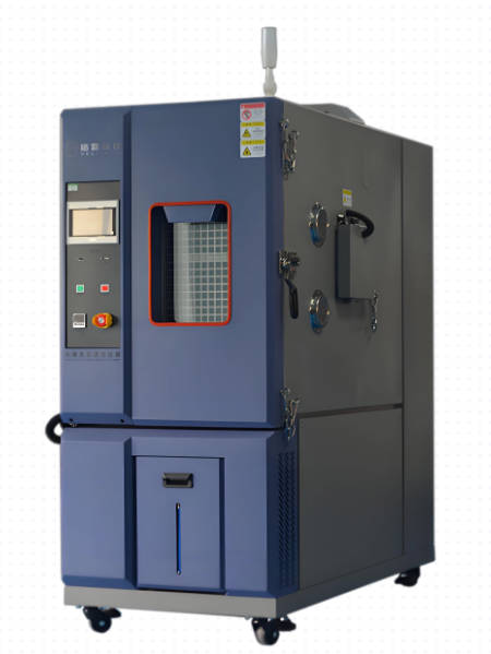
Response time is measured across temperature chambers (-55 °C to +125 °C and beyond), under controlled humidity, and at reduced atmospheric pressure to evaluate squeeze-film damping sensitivity. Long-duration endurance testing periodically samples actuation and release times over millions to billions of cycles, trending bounce growth and release time drift as early indicators of wear, contact material transfer, or stiction onset.
Statistical Process Control Analysis
Wafer-level probe stations with integrated switching time measurement channels collect lot-level data. Statistical analysis of response time distributions supports yield optimization, outlier screening, and correlation with process variables such as beam thickness and contact gap lithography.
Applications
MEMS metal contact response time testing supports quality assurance and design validation across multiple industries:
- RF and microwave systems: verification of switching speed in 5G/6G antenna routing matrices, beamforming networks, and reconfigurable RF front-ends where latency budgets are measured in microseconds.
- Automatic test equipment (ATE): qualification of MEMS relays in semiconductor test instrumentation, matrix cards, and parametric measurement units requiring fast, bounce-free switching.
- Aerospace and satellite payloads: validation of MEMS switches in reconfigurable payloads, redundancy switching, and phased array systems exposed to radiation and thermal cycling.
- Automotive electronics: response time confirmation for MEMS switching devices in battery management, sensor bus isolation, and safety-critical interrupt functions.
- Optical communication: characterization of MEMS-driven latching switches and bypass protection elements where electrical contact response contributes to protection switching time.
- Metrology and instrumentation: calibration laboratories and component manufacturers using standardized response time measurement to certify datasheet specifications and incoming inspection compliance.
FAQ
What is a typical response time for MEMS metal contact switches?
Most electrostatically actuated ohmic MEMS switches achieve actuation times between 1 and 100 microseconds, with optimized designs reaching sub-microsecond operation. Release times are generally shorter, often below 10 microseconds, since the restoring spring force acts immediately upon drive removal.
Why is contact bounce significant in MEMS metal contacts?
Although MEMS structures are small, the closing contact can still rebound several times before settling, generating intermittent resistance spikes and electrical noise. Extended bounce reduces usable switching speed in applications, accelerates contact erosion under hot-switching conditions, and is therefore a mandatory measurement item.
How does testing distinguish mechanical delay from contact formation delay?
Electrical probing measures the combined result, while laser vibrometry independently tracks mechanical displacement. Comparing the two timelines separates beam transit delay from contact interface effects such as surface film breakdown or micro-asperity deformation.
Can response time testing detect reliability problems early?
Yes. Progressive increases in release time often precede stiction failures, growing bounce durations indicate contact surface degradation, and actuation time drift can reveal charging of dielectric layers or hinge fatigue. Trending these parameters over endurance cycling provides leading indicators of impending failure.
What environmental factors most influence MEMS contact response time?
Ambient pressure strongly affects squeeze-film damping—lower pressure reduces damping and can shorten switching time but may worsen impact bounce. Temperature changes alter spring stiffness and gas viscosity, while humidity and contamination influence contact resistance formation dynamics. Comprehensive testing therefore includes environmental conditioning.
Is wafer-level response time testing feasible before packaging?
Yes. Probe-based switching time measurement on PCM structures allows response time screening at the wafer level, provided electrostatic actuation is compatible with probing conditions. Package effects such as residual gas composition and lid stress are then confirmed through final device-level testing.